
Wafer Inspection Machines: How They Work
Defect detention via automated vision inspection plays a key role in the manufacturing industry. They are crucial to sense, quantify, and correct defects in different devices.
As technology continues to advance, manufacturers are working towards achieving zero tolerances to defects in components and finished devices.
More AOI solutions are being developed to correct defect types in particles, crystals, at the noise level of their operating principles.
Wafer inspection machines are categorized into two: non-patterned wafer inspection machines and patterned wafer inspection machines.
In this post, we highlight a brief description of the wafer inspection machine or system and discuss how it works.
A wafer defect inspection system is a machine that can detect small defects and pinpoint the coordinates of the defects automatically which produces highly reliable and consistent results.
Wafer inspections are important to detect defects such as scratches, exposure problems, wafer edge flaws, spin defects, hot spots, particle contamination, and a wide range of other defects that may reduce chip performance.
If defects are not eliminated or filtered immediately, such defects may escape pass through the final testing. The implication is that valuable time and resources have been wasted. Flawed products can reduce the durability and lifespan of the device.
Types of Defects
There are two major types of defects that can be detected by wafer inspection machines. They are:
a. Systematic Defects
This kind of defect is caused by the conditions of the mask and exposure process; they will occur in the same position on the circuit pattern of all the dies projected.
Systematic defects occur in locations where the exposure conditions are difficult and require fine adjustment. Sometimes, systematic defects cannot be detected using a conventional inspection system.
b. Random Defects
This type of defect is caused by particles that become attached to a wafer surface, so their positions cannot be detected or predicted.
The wafer defect inspection machine’s major role is to detect defects on a wafer and obtain their position coordinates.

Non-Patterned and Patterned Wafer Inspection
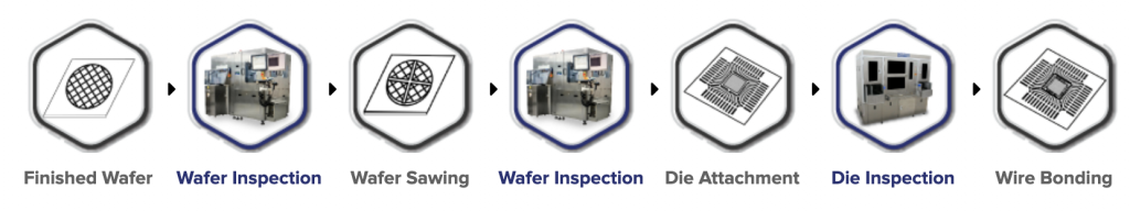
Unpatterned wafers inspection system is commonly used in the early stages of the semiconductor processes whereas Patterned wafer inspection is mostly used to detect defects on processed wafers.
Bare wafers are visually uniform across their surface compared to patterned wafers which have some patterns on them.
Wrapping Up
To provide precise and reliable results when detecting minor or major wafer defects, High-Performance Wafer AOI Solutions (Alpha Series) can be employed.
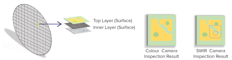
Cortex Wafer AOI can support different types of inspection depending on the processes the wafer goes through. Inspection can be done after the etching process, sawing process or before die attachment process.
This technology is supported by various types of wafer and is used in semiconductor, automotive, electronics, medical & optoelectronic industries.
Moreover, it now comes with a new SWIR camera-inner layer inspection for higher efficiency. Other key features include colour camera and mono camera.
For more information, feel free to get in touch with our AOI solution specialists for a full consultation.