
What is SWIR and Its Application to AOI
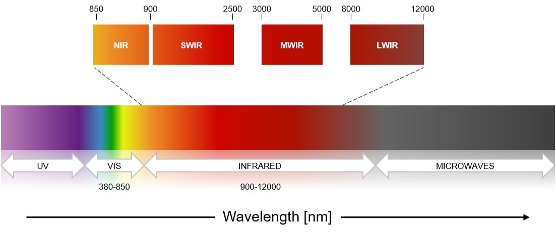
SWIR (Short-wave infrared) light is defined as light within the spectral band 0.9 – 2.5μm. SWIR lies between visible and thermal imaging which gives it its unique properties.
Its proximity to the visible range gives it all its imaging qualities in terms of resolution and contrast, and at the same time, its infrared spectrum allows it to unveil elements that are not visible to the naked eye. Such high-quality imaging technology requires unique optical and electronic components capable of covering the typical SWIR range.
InGaAs (Indium gallium arsenide) sensors are the primary sensors used in SWIR imaging and are divided into linear line-scan InGaAs and area-scan InGaAs sensors. These are powerful, controlled, and camera-adapted light flux that can overcome the current limits of lighting in industries.
While area-scan InGaAs sensors are typically ITAR restricted, linear line-scan inGaAs sensors are commercially available. In case you are wondering, ITAR (International Treaty and Arms Regulations) is a regulation enforced by the US government, which ensures products must adhere to strict import and export regulations for them to be manufactured or sold inside or outside the United States.
With proper licenses, SWIR inspection can be used for numerous commercial applications.
SWIR Applications
SWIR inspection is used in a wide range of applications including solar cell inspection, surveillance, electronic board inspection, process quality control, produce inspection, anti-counterfeiting, identifying and sorting, and so on. Below are some of its applications.
- Highlight the presence of a contaminant inside a solid, liquid, or bubbles
- Detect, identify, and differentiate elements that are transparent or identical in the visible range
- See writings through plastics that are not visible to the human eye
- Detect and control solid/liquid filling level inside a plastic container
- Check the presence of internal parts, as a gasket.
Cortex Robotics AOI solution with SWIR Application
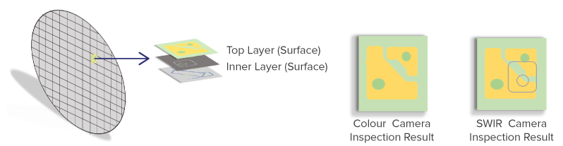
The inner or side wall wafer defects causes by stress at different stage of the manufacturing process is not easily detected or be seen by visible inspection. The undetected defects might cause the electronic circuit from operating correctly, thereby making the products as a defective product leading to premature failure.
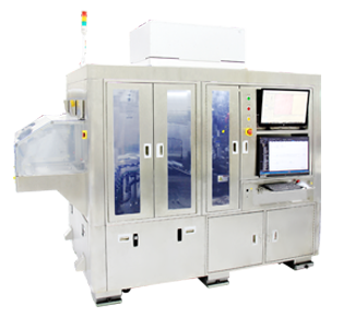
Cortex Robotics Wafer & Die AOI solution is a high-performance SWIR wafer inspection machine that supports the backend of the semiconductor manufacturing process. This highly-rated AOI machine automatically detects minor or major wafer defects including inner and sidewall cracks while providing precise and reliable results.
SWIR Unique Features
- SWIR is designed in such a way that water vapour, collagen, fog, lipids, and certain materials such as silicon (that are impossible or difficult to perform using visible light) are transparent or revealed.
- SWIR has a different wavelength that is invisible to the human eye.
- SWIR wavelengths transmit through lenses, glass, and other optical components (including windows, optical filters, etc.) to see through opaque materials such as plastics and silicon whether it is in the day or at night.
- They can penetrate the inner layer of a particular layer depending on the object.
- SWIR features a wafer that is built with many layers. As it gets thinner, the handling becomes difficult and easily causes defects. A crack within the inner layer might reduce its ability to detect by normal inspection.
Our AOI solutions support various types of wafer inspection in various types of industries such as the semiconductor, automotive, electronics, as well as in medical and optoelectronic industries.
Wrapping Up
SWIR is an added point to AOI solutions, making it the future of inspection. When used for inspection, quality control, surveillance, sorting, and other relevant applications, SWIR imaging boasts numerous advantages over the visible spectrum.
Manufacturers recommend that users choose components that are specifically designed, optimized, and coated for the SWIR wavelength range. This is to ensure low optical aberrations and the highest resolution images. Using a lens designed for visible imaging will result in higher aberrations and lower resolution images.
Cortex Robotics, a specialist in AOI solutions and equipment for demands across various industries, possesses the SWIR technology for wafer inspection. For further information, please feel free to get in touch with our consultants.