
Description
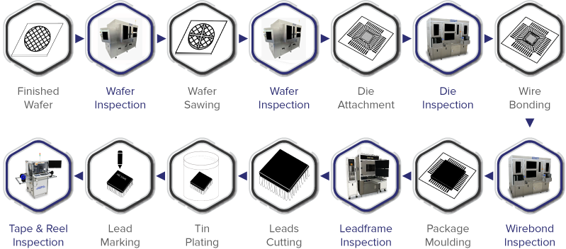
我们的 AOI 解决方案支持半导体后端制造流程
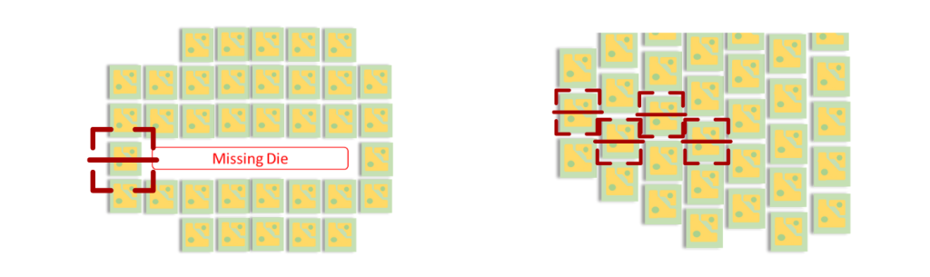
成品晶圆

晶圆检测
晶圆切割

晶圆检测
贴片
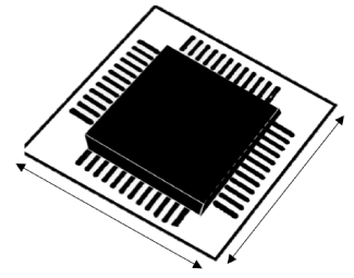
芯片检测
引线键合
卷带检测
转塔式集成电路检测
打标
切筋成型
导线框检测

注塑成型
焊线检测
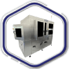
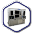
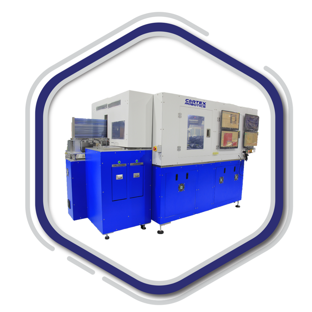
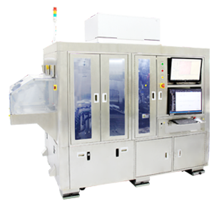
阿尔法系列
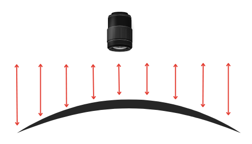
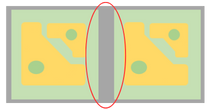
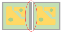
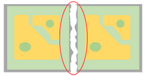
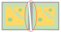
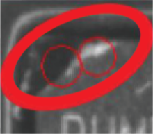
高性能晶圆切割前后检测
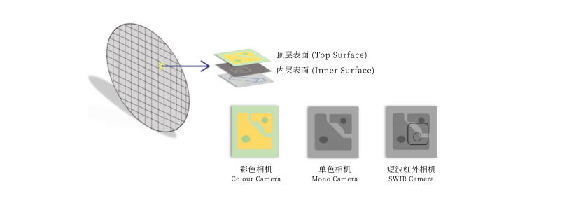
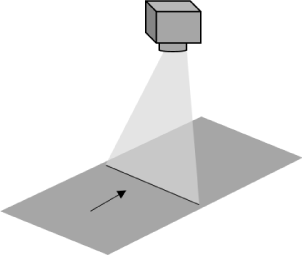
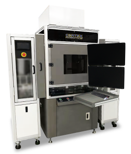
阿尔法系列是高性能晶圆 AOI 解决方案。这些先进的系统旨在自动识别和分类晶圆切割过程后出现的主要和次要缺陷,从而提供可靠且高度准确的缺陷分析。 我们的晶圆 AOI 系列的最新版本引入了 SWIR 技术,检测能力显着增强。 这种短波红外技术已被集成到系统,能够检查半导体芯片的内层和侧壁,从而增强了我们检测这些关键区域的缺陷的能力。 这种基于 SWIR 的新型晶圆检测解决方案得到了升级硬件和软件组件的支持,旨在优化和加快晶圆转换和检测流程。
AOI 检测优点
给商务

完整解决方案检
查、标记、排序

提高质量
快速识别和修复缺陷流程

提高公司声誉
减少产品缺陷可提高客户满意度

减少浪费
可以在早期阶段发现缺陷

节省时间和成本
流程可以简化并减少劳动力成本

24小时运作
提高产量
给用户

检查覆盖各单位产
品不容错过

数据采集
启用跟踪和数据分析

一台AOI机
多种缺陷检测

方便使用
简单的说明手册,带有自己的配方设置

可靠的结果
一致的检验标准

100% 自动化流程
替代人工检查
特点
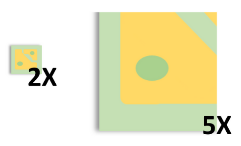
最小缺陷检测尺寸 - 0.5um

最小芯片检测尺寸300umx300um

自动聚焦(产品翘曲补偿)

可以适应晶圆图档 (比如Klarf, XML等)

实时检测结果显示

自动晶圆图定位

二维读码器

带电离空气和真空的自动门

SECSGEM 兼容

可选特点
去除模块

拒料前支持在线或离线验证

底部多视图检测

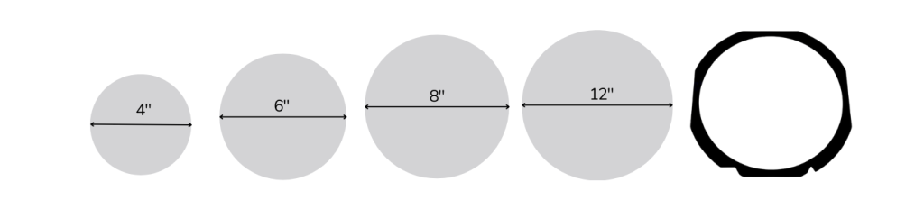
检测范围


*为了保护我们的客户设计,绘图仅用作说明目的。 联系我们获取更多信息
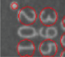
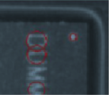
ELECTRA SERIES
Tape & Reel AOI Solutions
Electra is a powerful High-Speed Tape and Reel AOI Solutions that is capable to inspect fine defects.
Its support various pocket width of tape and reel.
BENEFITS OF AOI INSPECTION
To Business
Full Solution
Check, Mark, Sort
Increase Quality
Quick identify & Fix defects process
Improve Reputation
Less defects products increase
customer satisfaction
Reduce Wastage
Defects can be detect at the earlier
stage
Save Time & Cost
Process can be simplify and less
labour cost
24 hours operation
Maximize production yield
To User
Inspection cover each unit of
products without miss
Data Collection
Enabling tracking & data analysis
One AOI Machine
Multiple types defects inspection
Easy Control
Simple Instruction manual with
own recipe setting
Reliable Result
Consistent inspection criteria
100% Automatic Process
Replace manual inspection
Key Features
Dual Track Operation
Autosave failed defect images
Fine detection to 4 mils defects
Line Scan 8K, 12K, 16K Camera Capabilities
Other Features
Single software with multiple inspection recipe

Network connectivity for output to server

Defect mapping with images

Optional Features
Laser marking system

Offline Programming

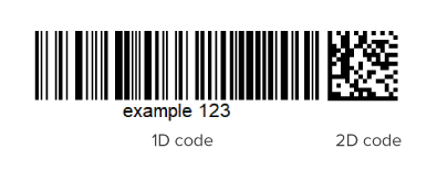
2D code reading
NAS Storage Solution

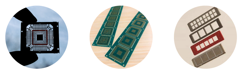
INSPECTION PRODUCTS
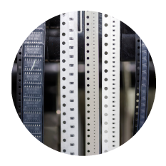
Tape & Reel
INSPECTION CAPABILITIES
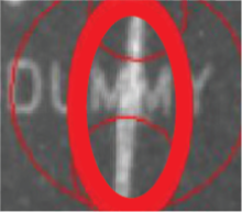
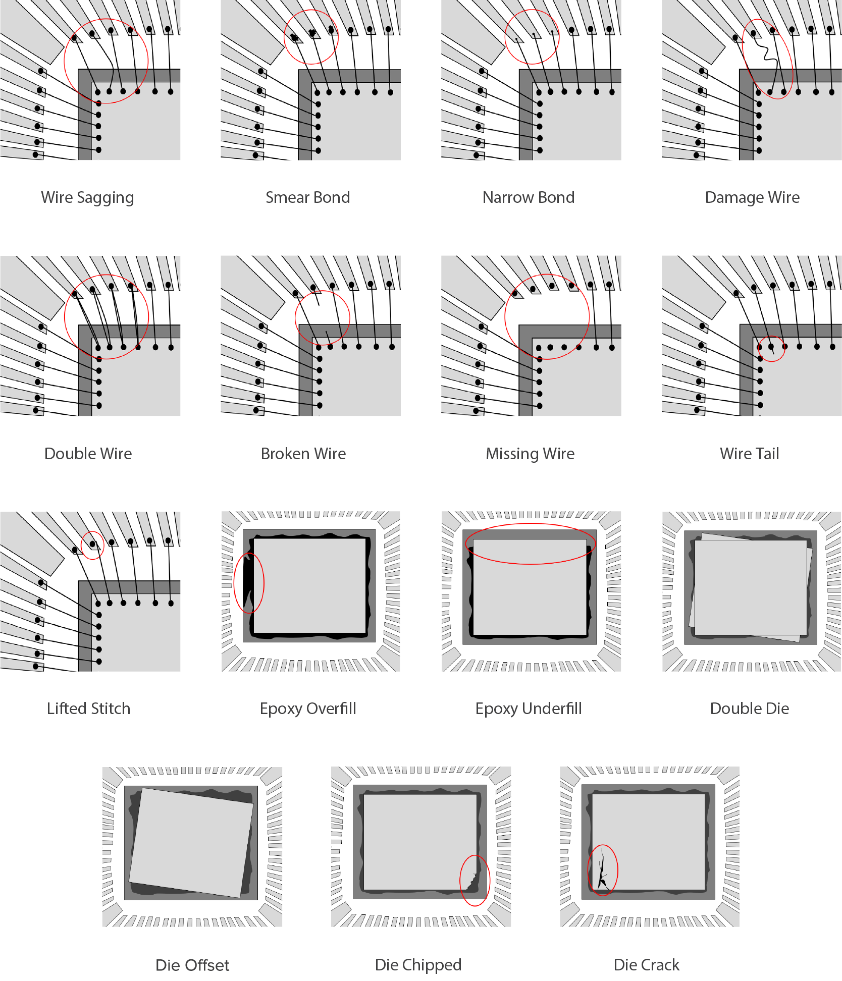
Scratches, chipping, wrong marking, wrong orientation, foreign material and lead bend
Scratch
Chip Out
Wrong Marking
Wrong Orientation
Foreign Material
Lead Bend
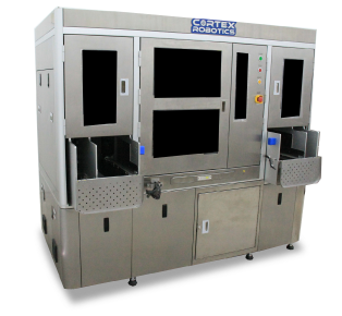
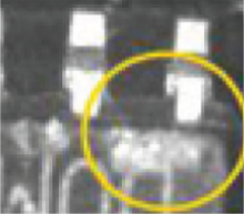
VEGA SERIES
High Precision 3D Wirebond AOI Solution
Vega is a High Precision Wire bond Inspection (AOI) solution equipped with the latest & high-specification 3D technologies which able to perform a smarter and high accuracy height measurement inspection on the die and on wirebond. It’s designed to support inspection before and after the wire-bonding process. It has the capability to inspect the top and bottom of the 3 types of products (Leadframe, Substrate & Pallet) with only a few steps of recipe change. The 3D Wire Bond Inspection has the ability to detect not only the common wire bond defect but also defects such as wire drop, die tilt, and more. It comes with a multi-choice of reject modules that suit your need, for example, laser marking, laser cutting, inking, and Pick&Place.
BENEFITS OF AOI INSPECTION
To Business
Full Solution
Check, Mark, Sort
Increase Quality
Quick identify & Fix defects process
Improve Reputation
Less defects products increase
customer satisfaction
Reduce Wastage
Defects can be detect at the earlier
stage
Save Time & Cost
Process can be simplify and less
labour cost
24 hours operation
Maximize production yield
To User
Inspection cover each unit of
products without miss
Data Collection
Enabling tracking & data analysis
One AOI Machine
Multiple types defects inspection
Easy Control
Simple Instruction manual with
own recipe setting
Reliable Result
Consistent inspection criteria
100% Automatic Process
Replace manual inspection
Key Features
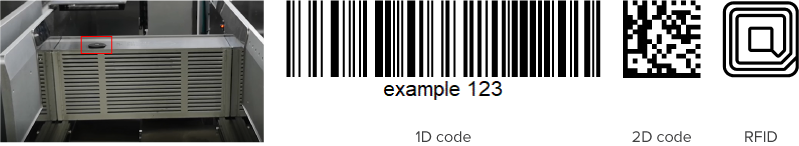
Multiple Magazine Conveyor
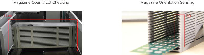
1D / 2D / RFID Magazine Reader
Other Features
Quality Analysis System

Generate Report

E-Map

High-Resolution Camera & Auto focusing

8 to 1 Centralised Verification System

SECSGEM Compatible

Auto frame width Adjustment

Able to perform offline verification before reject

Optional Features
Reject Modules (inking, sorter & laser marking)

Bottom inspection

Long Term Storage (up to 3 months)

Offline Teaching
INSPECTION PRODUCTS
Substrate, Leadframe and Pallet
INSPECTION CAPABILITIES
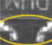
Wire short, wire broken, wire sagging, wire sweeping, torn bond, wire missing, double-bond, lifted wire, lifted ball, ball dimension, particle on die, die off set, epoxy overflow, lead bent, lifted stitch
MIRA SERIES
Strip to Strip AOI Solutions
Mira is a High-Speed Strip to Strip AOI solution with multiple inspection capabilities and low energy consumption solutions.
Its also able to do inspection on die attached and various types of leadframe and package.
BENEFITS OF AOI INSPECTION
To Business

Full Solution
Check, Mark, Sort

Increase Quality
Quick identify & Fix defects
process

Improve Reputation
Less defects products
increase customer
satisfaction

Low Energy Consumption
For greener earth

Reduce Wastage
Defects can be detect
at the earlier stage

Save Time & Cost
Process can be simplify and
less labour cost

24 hours operation
Maximize production yield

RoHS Compliance
Component
To User
Inspection cover each unit of
products without miss
Data Collection
Enabling tracking & data analysis
One AOI Machine
Multiple types defects inspection
Easy Control
Simple Instruction manual with
own recipe setting
Reliable Result
Consistent inspection criteria
100% Automatic Process
Replace manual inspection
Key Features
Dual Scan Capabilities Top & Bottom Inspection
1D & 2D Reading
Fine detection to 2 mils defects
Line Scan 8K, 12K, 16K Camera Capabilities
Other Features
Single software with multiple inspection recipe
Network connectivity for output to server
Defect mapping with images
Optional Features
Laser marking system
Able to perform offline verification without disturbing the on-going process
NAS Storage Solution
INSPECTION PRODUCTS
Package, Leadframe, Die Attach
INSPECTION CAPABILITIES
Mark & Cosmetics inspection – Rough surface, void, package scratches, incomplete fill, crown flash (2D), ID Pin Height, Chip on package, raised flag, package offset, foreign material, pin1 chip, flash on EP and etc